
The CPU landscape is evolving and undergoing a major transformation—from the conventional single-die approach, where all components were tightly integrated together, to today’s groundbreaking chiplet-based architectures, where CPU dies and the I/O die are decoupled yet assembled like precision-engineered building blocks. This post delves into the latest developments in CPU technology and explores the fundamental architectural changes shaping the next generation of computational power.
Let’s take a closer look at what makes these chiplet-based designs faster, more efficient, and fundamentally different from traditional CPUs.
Traditional CPU architecture
Transistors are the fundamental building blocks of processors. Over the past 55 years—and as illustrated by the Moore’s law (see e.g. here)—CPUs have evolved from containing just thousands of transistors to integrating billions on a single chip, representing a million-fold increase. At the same time, transistor sizes (see Fig. 1) have scaled down dramatically, shrinking from micrometers to nanometers and driving a 10,000-fold revolution in miniaturization.
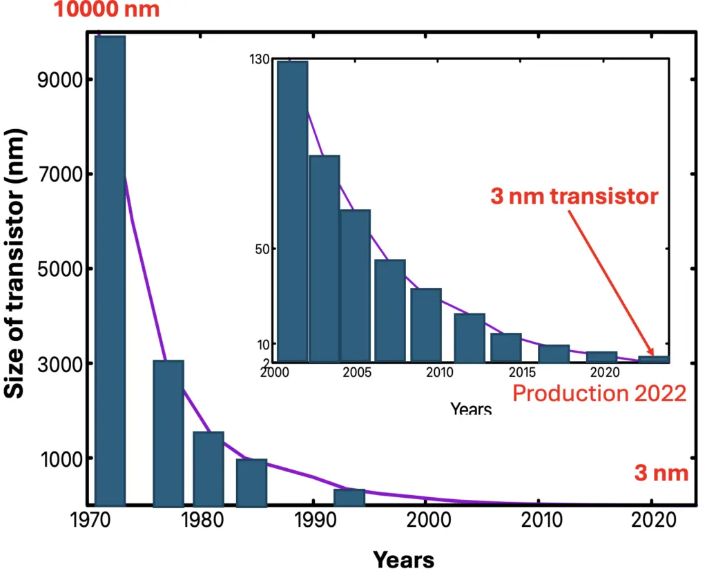
Fig. 1. Evolution in transistor size in the last 55 years. Data is taken from here
Traditional single-socket CPU processors typically comprise one CPU die with up to 64 cores. Figure 2 shows a simplified dual-CPU system diagram (two sockets), highlighting the memory hierarchy and its key components:
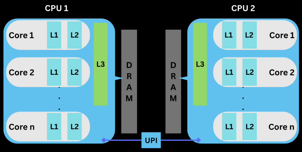
- CPU 1 and CPU 2: Two distinct Central Processing Units, indicating a multi-processor system.
- Cores (Core 1, Core 2, …, Core n): Each CPU comprises multiple processing cores, each capable of independently executing instructions.
- L1 and L2 Caches: Each core has its own private L1 and L2 caches. These are small, fast memory components that store frequently accessed data, reducing the need to access slower main memory (DRAM). L1 is typically faster but smaller than L2.
- L3 Cache: Each CPU has a shared L3 cache (or multiple L3 caches), serving a group of cores that constitute a NUMA node or domains (Non-Uniform Memory Access). In a NUMA-based system, cores on each CPU are grouped into nodes (e.g. 4 NUMA nodes see here)—each with its own shared L3 cache—linked via a cache-coherent interconnect. The L3 cache is a larger, slower cache shared by a group of cores within the same CPU. It acts as an intermediary between the L1/L2 caches and the main memory.
- DRAM: Dynamic Random Access Memory, representing the main system memory. It’s the primary storage for data and instructions that the CPUs are actively using.
- UPI (Ultra Path Interconnect): This represents the high-speed interconnect between the two CPUs. It allows for efficient communication and data sharing between the processors, crucial for maintaining cache coherence and overall system performance in a multi-processor environment.
This traditional architecture is commonly found in servers and high-performance workstations. It highlights the importance of caches in reducing memory latency (i.e., the time it takes to access data from memory) and the role of the UPI in enabling inter-processor communication.
Modern CPU architecture— the AMD chiplet model
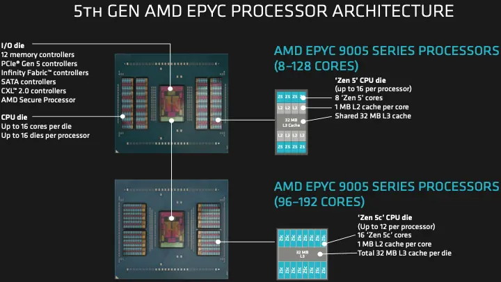
In traditional CPU designs, the CPU cores, memory controllers, PCIe controllers, and other components are integrated on the same die. This monolithic approach limits both core scalability and design flexibility, as increasing the number of cores or upgrading specific components often necessitates redesigning the entire chip. AMD introduced a breakthrough with its chiplet-based architecture (cf. Fig. 3), which decouples the CPU compute dies (CCDs) from the I/O die and connects them using AMD’s Infinity Fabric. This hybrid multi-chip design is exemplified by the 5th Gen AMD EPYC 9005 CPU, in which:
- CPU cores reside on dedicated chiplets (CCDs).
- I/O functions (memory/PCIe controllers) operate on a separate I/O die.
Figure 3 presents the two latest AMD EPYC processor designs— hybrid multi-die architectures. It shows two product configurations of the 5th Gen AMD EPYC 9005 CPU architecture: (i) ‘Zen 5c‘ CPU die and (ii) ‘Zen 5‘ CPU die produced using 3nm and 4nm process technologies, respectively. Let’s take a closer look at various components of these multi-chips processors, specifically focusing on the ‘Zen 5c‘ CPU die.
CPU Die
The architecture of the AMD EPYC 9005 series processors (TURIN – ‘Zen 5c‘ core) is known for their high core counts ranging from 96 to 192 cores per processor. The processor is composed of multiple ‘Zen 5c’ CPU dies, with up to 12 dies in a single processor. Each of these dies contains 16 ‘Zen 5c’ cores. Furthermore, each core is equipped with 1MB of L2 cache, and each die features a total of 32MB of L3 cache (max of 512 MB) shared among its 16 cores.
I/O Die
The I/O die is a dedicated die and acts as a central hub for managing data flow in and out of the processor, ensuring efficient communication with CPU dies. The I/O die houses several key controllers, and here we provide a short description of each components (further details can be found here) :
- 12 memory controllers: It features 12 memory channels with a max per-socket theoretical bandwidth of 614 GB/s. The processor supports a max memory capacity of 6TB DDR5-6400 (see p. 7 of the white paper).
- PCIe Gen 5 controllers: These provide high-bandwidth lanes for connecting to external devices such as graphics cards, network adapters, and high-speed storage.
- Internal Infinity Fabric: This connects the I/O die to each CPU die. The I/O die has up to 16 Infinity Fabric connections to CPU dies per AMD EPYC processor—a total bandwidth of 72 GB/s (or 16×36 Gb/s Infinity Fabric links) (see p. 10 of the white paper).
- AMD Infinity Fabric: These are essential for inter-processor communication (e.g. between 2 physical sockets). Each PCIe link (having 16 lanes) has a total bandwidth of 64 GB/s. The system supports the use of three or four PCIe links. When four links are configured, they can support a maximum theoretical bandwidth of 512 GB/s between processors (see p. 11 of the white paper).
- SATA controllers: These are present for connecting to traditional SATA-based storage devices. SATA (Serial ATA) is a computer bus interface used to connect storage devices like hard drives (HDDs) and solid-state drives (SSDs) to a computer system.
- AMD Secure Processor: Finally, this provides hardware-level security features. It manages coordination between CPU cores, memory controllers, and boot firmware e.g. memory encryption mechanisms (see p. 14 of the white paper).
Conclusion
The innovative design of modern AMD high-performance processors, characterized by the decoupling of the CPU die from the I/O die, enables: (i) independent optimization of each die; (ii) the creation of diverse product configurations (an example is illustrated in Figure 3); and (iii) the elimination of external chipsets by integrating multiple functions within the I/O die. On the other hand, the high-density design with numerous cores and a large amount of cache, makes the AMD EPYC 9005 series processors well-suited for AI-enabled workloads and enterprise computing.
References
- 5th Gen AMD EPYC Processor Architecture (white paper): https://www.amd.com/content/dam/amd/en/documents/epyc-business-docs/white-papers/5th-gen-amd-epyc-processor-architecture-white-paper.pdf
- 5th Generation AMD EPYC™ Processors (main website): https://www.amd.com/en/products/processors/server/epyc/9005-series.html
- Types of CPUs: https://www.ibm.com/think/topics/central-processing-unit-types
-
The Exascale Era: From Megaflops to Exaflops:
The Exascale Era: From Megaflops to Exaflops
- Overview of Compute Node Diagram: https://docs.olcf.ornl.gov/systems/frontier_user_guide.html
- NUMA Architecture: https://learn.microsoft.com/en-us/windows/win32/procthread/numa-support
- Architecture of HPC systems: https://github.com/HichamAgueny/HPC_architecture